Design & Engineering Services
DFM Review · PCB Design Support · Prototype Builds
Design & Engineering at Vishesh, Bangalore
Most design problems that reach the production line were preventable. Vishesh's design and engineering services exist to catch them earlier — reviewing your layout for manufacturability, optimising your BOM for real-world availability, and building your first prototype on the same lines that will run your production. One team, one facility, no translation loss between design and manufacture.
Vishesh's design and engineering support is part of a fully integrated electronics manufacturing services operation from its 45,000 sq ft facility at Gottigere, Bangalore. DFM reviews are grounded in real process constraints from our Siemens SMT assembly lines — not theoretical guidelines. Every prototype build runs on the same production lines, under the same ISO 9001:2015 and IATF 16949:2016 certified quality system, issued by TÜV Rheinland.
Manufacturing-Aware Engineering Support
Four services designed to close the gap between your design and a production-ready board.
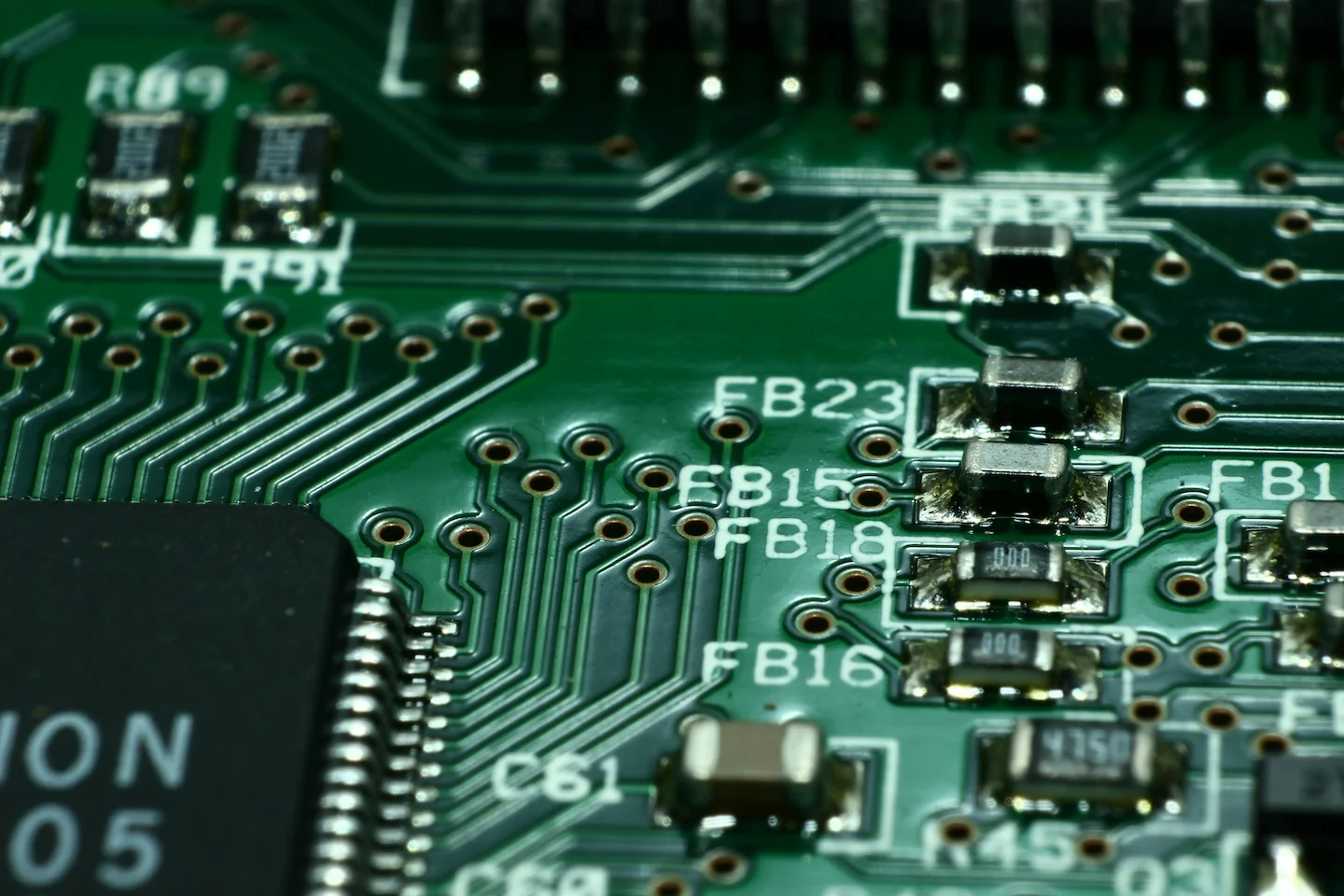
DFM Review
We review your Gerber files and design against our SMT and THT process capabilities — flagging issues before they become production defects or costly redesigns. Report returned within 3 business days.
PCB Design Support
Layout guidance, stack-up review, component placement optimisation, and design rule checks aligned to IPC-certified standards and our manufacturing process.
BOM Optimisation
Component availability review, alternate part identification, and cost optimisation — so your BOM is production-ready before your first order.
Prototype Build & Validation
First-article builds on our PCB assembly lines with full inspection — AOI and X-ray where required — so design issues surface at prototype stage, not at volume.
From File to First Build
Every DFM review and prototype build at Vishesh follows a documented, repeatable process — from file submission through to first-article sign-off.
Share your Gerber files, BOM, and any design notes via the form below.
- Gerber files (RS-274X format), drill files, and BOM required
- NDA available before any files are shared or reviewed
Our engineering team reviews your design against Vishesh's manufacturing capabilities.
- DFM report with specific findings and recommendations returned within 3 business days
- Reviewed against real SMT, THT, and wave soldering process constraints — not guidelines
Once design is validated, we build your prototype on the same SMT lines used for production.
- First-article builds with 100% AOI and X-ray inspection where required
- Design changes are fast — reviewing and building under one roof
What Vishesh Can Support
| Capability | Detail |
|---|---|
| DFM review | Gerber file review against SMT, THT, and wave soldering process capabilities |
| PCB design support | Layout guidance, stack-up review, IPC-compliant design rules |
| BOM optimisation | Component availability, alternate part identification, cost review |
| Prototype build | First-article SMT builds with AOI and X-ray inspection |
| Component range | 0201 to BGA, LGA, CSP — fine pitch 0.3mm |
| PCB complexity | Up to 16-layer boards |
| Inspection | 100% AOI + X-ray (Unicomp AX-7900) on prototype builds |
| Standards | IPC-certified trainer on-site, IPC-2221 design rule compliance |
| Turnaround | DFM report within 3 business days of file submission |
| Facility | 45,000 sq ft, Bangalore — same facility used for production |
Vishesh's Plant 1 handles all PCBA and testing. Every prototype build runs on the same Siemens SMT lines used for production — so DFM feedback is grounded in real process constraints, not theoretical guidelines. For a full overview of Vishesh's manufacturing capabilities, visit our PCB assembly services page.
Why Choose Vishesh for Design & Engineering?
DFM reviewed by the team that builds it — your design is assessed against the actual Siemens SMT lines and process parameters used in production, not against generic guidelines.
Prototype to production without changing supplier — your prototype runs on the same equipment, the same quality system, and the same floor as your production volume. No translation loss between runs.
3-day DFM report turnaround — specific findings with actionable recommendations, not a generic checklist. For urgent programs, contact us to discuss an accelerated timeline.
IPC-certified trainer on-site — design rule checks are aligned to IPC-2221 and enforced at operator level. ISO 9001:2015 and IATF 16949:2016 certified by TÜV Rheinland.
NDA available before file submission — your design remains confidential. Contact us to arrange an NDA before sharing any technical files.
Frequently Asked Questions
What files do I need to submit for a DFM review? +
Submit your Gerber files (RS-274X format), drill files, and BOM. A schematic in PDF is helpful but not required for the initial review. If you have specific concerns about your design, note them in the submission form — our engineers will address them specifically in the DFM report.
How long does a DFM review take? +
We return a DFM report within 3 business days of receiving complete files. For urgent programs, contact us directly and we will confirm if an accelerated timeline is possible.
Is my design kept confidential? +
Yes. An NDA is available before any files are shared or reviewed. Contact us to arrange this before submission if required.
Can Vishesh help if my design is already in production but having quality issues? +
Yes. We can review an existing design for process-related quality issues — pad geometry, thermal relief, component clearances, and soldering profile compatibility. This is often faster than a full redesign and identifies the specific changes needed to resolve production defects.
Does Vishesh provide full PCB schematic design or only DFM review? +
Our primary service is manufacturing-aware design support — DFM review, layout guidance, BOM optimisation, and prototype builds. For full schematic design from concept, contact us to discuss your requirements and we will assess whether we can support your specific program.
Ready to Review Your Design?
Submit your Gerber files and BOM and our engineering team will assess your design for manufacturability. We return a DFM report within 3 business days — with specific findings, not generic feedback.
NDA available before file submission
DFM report within 3 business days
Same team reviews your design and builds your prototype